Let's get acquainted with the Intel H55 Express using the example of the ASRock H55M Pro motherboard. Expansion cards and video controllers
Noticed a mistake? Select a piece of text and press CTRL+ENTER!

It is obvious that the Intel H55 chipset has gained great popularity among users and motherboard manufacturers, because none of the Intel chipsets with an integrated graphics core have ever been presented in so many different modifications. Technically, the graphics core is now found in every Intel processor for the LGA 1156 platform, but in practice it can only be used on boards based on Intel H57, H55, Q57 and Q55 chipsets. However, the Intel HD Graphics video turned out to be quite successful and modern, and besides, we repeat, every processor of the Westmere family has it, so the temptation to use it is quite strong.
The first board we reviewed that can use the Intel HD Graphics core was the ASRock H55M Pro. Despite the fact that the product is made in Micro ATX format, the H55M Pro is a fairly functional solution with its own characteristics. Such as, for example, two slots for video cards. The ASRock H55M Pro should be considered a functional media center or a powerful entertainment PC; fortunately, the board has the necessary set of outputs and interfaces for this purpose. But today we are not talking about her. ASRock has already released more than 10 products based on the Intel H55 chipset. Today we will look at the younger model - ASRock H55M-LE, which would be more appropriate in an office or relatively inexpensive home PC.
Specifications
Since the ASRock H55M-LE is designed to build affordable PCs, the developers have done without unnecessary frills. The main functionality of the board is provided by the capabilities of the Intel H55 chipset. Additionally, only a PCIe gigabit network controller and an eight-channel HDA codec were required, which is practically a de facto standard today.

Design and Layout

The only complaint that can be raised is the fact that there are two slots for RAM, which will definitely create problems when upgrading - simply adding a couple of modules will not work here. However, practice shows that for the entire life cycle Most systems never “wait” for an upgrade.

It’s very interesting that the board’s specifications state support for enormous high frequencies, up to DDR3-2600, however, only in overclocking mode, but this is understandable.
Meanwhile, the board is also captivating with its traditionally well-thought-out arrangement of elements. All connectors to which any cables are connected are soldered to the sides of the PCB. No incompatibilities in the relative arrangement of slots and connectors were also noticed.

Recently, when it comes to products that will potentially be used in offices and, possibly, industrial desktops, there has been a trend towards conscientious implementation of connectors for connecting COM and LPT ports. On the ASRock H55M-LE, the corresponding headers are placed in close proximity to the logical location of the brackets with the physical implementation of the ports. As practice shows, while these archaic interfaces are not used at home except for specific tasks such as firmware for some devices, quite a lot of equipment is still produced and sold for industry, one way or another using COM or LPT.

With slots for additional devices, the ASRock H55M-LE is still quite simple. In addition to the unchanged PCI Express 2.0 x16, the implementation of which is not neglected even on ultra-compact boards for HTPC, there are two more PCI and one PCI Express 2.0 x1.

The processor power supply voltage regulator has four PWM phases. The element base in this case can be called classical, because the circuits use ordinary field-effect transistors (MOSFETs), chokes and polymer capacitors. The circuit is controlled by a Richtek RT8857 PWM controller.

We have not seen this chip before, but judging by technical specifications, this is a completely modern and functional four-phase controller, two channels of which are provided with built-in MOSFET drivers.

Here we note that ASRock still pays a lot of attention to ease of upgrade and compatibility, so the ASRock H55M-LE PCB, like other company products for the LGA 1156 platform, has four additional holes that can be used to install coolers equipped with mounts for LGA 775. By the way, very convenient. After all, LGA 1156 was the last to be announced, so it happens that many not-so-new multi-platform cooling systems are compatible even with LGA 1366, but “don’t know” about LGA 1156.

The single chip of the Intel H55 chipset is cooled by a small needle-shaped aluminum alloy heatsink. Considering the heat generation of this crystal, this is quite enough for it.

The board's input/output panel looks quite adequate to the functionality of the product. Obviously, to complete the picture, there is not enough HDMI connector, but the DVI present here can easily be converted into it. To convert the output to HDMI 1.3 with support for Full HD, Deep Color, xvYCC and HBR audio, only a passive adapter will be enough.

It is also important that on the surface of the ASRock H55M-LE there are jumpers that can be used to turn off the power supply to the USB ports in standby mode, which allows you to save energy and avoid the sometimes annoying glow of the LEDs of USB devices when the computer is not in use.
The ASRock H55M-LE BIOS is based on AMI microcode. The setup utility screen greets us quite detailed information O current version BIOS, model installed central processor and its main technical characteristics, as well as memory modules and the mode in which they operate.

Before testing began, the board's basic I/O system was updated to the latest version at the time of testing - 1.6, dated September 2010. It is obvious that ASRock pays great attention to supporting its products, which can be seen at least from the constant BIOS updates. ASRock offers several options for the procedure for changing the board firmware, but it’s very good that among them there is the most adequate and convenient way- using the appropriate flash driver contained in the BIOS itself. Using the ASRock Instant Flash option, you can update the firmware from a number of media, including USB flash drives, bypassing any operating systems.


At the beginning of the section there are a number of sub-items with which you can overclock components to pseudo automatic mode, that is, using one of several overclocking profiles configured by the developers. However, the board is not deprived of all the necessary “manual” settings.
It is important that at the end of the “OC Tweaker” section there is the ability to save three profiles of settings made by the user.

The budget Intel H55 chipset, as one might expect, did not become a milestone in the development of the industry. However, it has attracted the attention of motherboard manufacturers to create inexpensive models, as it provides quite sufficient “average” functionality for today and fully implements the capabilities of the built-in video of new Intel processors. The reduced selling price of the chipset also came in handy. ASRock (probably the largest specialist in budget solutions) liked this combination so much that in its implementation we see for the first time something unprecedented: a board () on an integrated chipset that does not use the capabilities of integrated video. Of course, from an economic point of view, this is a completely justified decision, but, you see, it looks unexpected.
Today we will look at a much more ordinary solution. We are already familiar with the microATX model P55M Pro, and on the H55 its almost complete analogue is the subject of this test - the H55M Pro. This is by no means a junior solution in its line, but it fits well into the category of inexpensive boards. Let's see how ASRock specialists managed to balance the price and capabilities of the new model.
Features of the board
ASRock H55M Pro is the only one of the company's boards in the new line that uses the full (standard) width of the PCB. Other microATX models make do with a narrowed printed circuit board; fortunately, no one will demand rich expansion capabilities from budget solutions. It’s more interesting what exactly was sacrificed when designing the H55M Pro: space was found to implement FireWire, to retain all 4 memory slots, and even to install an “adult” 8-pin processor connector. But quite unexpectedly they abandoned FDD and, most incredibly, IDE. ASRock doesn’t allow itself such free-thinking even in top-end motherboards, but here the space was too tight. And to conclude the triumph of the absurd, on the PCB (although not on the rear panel) there are connectors for connecting COM and LPT ports on the brackets. So understand this mysterious East.
Apart from the noted oddities, the board layout does not contain any unpleasant surprises. The capabilities of the chipset are almost fully realized, and if, say, the second PCIEx16 slot is connected in reality to 4 PCI Express lines from south bridge(read, PCI-E 1.1), then the greed of the manufacturer is not to blame for this, but the limitation of the cheap Intel chipset. Of course, there is no question of SLI or even normal CrossFire, but the support for video accelerators integrated into low-end Core i5/i3 and Pentium G processors is excellent. The eSATA port is implemented in a “budgetary way”, due to the chipset port, but it has power lines (the so-called Powered eSATA). In general, the very low cost of this model should in no way be misleading: in terms of the range of features, the H55M Pro corresponds to a high-quality mid-level board. Well, the shortcomings are quite familiar and forgivable: assembling the computer is a little difficult due to the proximity and crowding of some connectors. 
The processor's switching voltage regulator uses a 4+1+1-channel design (4 channels for the core, 1 for the so-called Uncore logic, including the memory controller, and 1 for the built-in video accelerator). All single-channel converters (including the memory module power converter) use 4 field-effect transistors, and the processor core power circuit uses 2 per channel. This organization of the power subsystem claims to be standard in the lower class of modern motherboards, although for record overclocking it is clearly worth preferring a different model. In addition, in all circuits on the H55M Pro, only high-quality polymer capacitors made in Japan (Nichicon) are used, and this, although not a decisive advantage, is still an argument for good faith. During our standard test tests, in any case, no problems were identified in operation. 
As you can easily see from the photographs, ASRock engineers treated the cooling of the board components, let’s say, without fanaticism. The chipset has a decorative stand for a chip with the company name, and the processor power converter is completely left without additional attention. However, we have already noted more than once that motherboards for Socket 1156 (that is, based on low-power chipsets), with a sufficient number of field-effect transistors in the processor power circuit, usually do not have cooling problems. If you make sure that the processor cooler blows air towards the rear panel of the board, even at minimum speed, you can safely forget about cooling the board.
PWM processor power controller, as on all modern boards, implements technology for reducing the number of active channels in a voltage converter depending on the load. Some difference in the ASRock implementation is that the proprietary IES (Intelligent Energy Saver) technology can be enabled not only using the proprietary utility of the same name, but also from the BIOS Setup - then you will not need to run the utility under Windows, except for tracking state of the PWM controller. 
No more branded ones distinctive features the fee does not have. You can only remember the proprietary system for mounting a processor cooler - CCO (Combo Cooler Option), which allows you to use your favorite (or simply cheaper) cooler for Socket 775 on the ASRock H55M Pro. In this case, the cooler will have to be installed with a slight rotation relative to the standard mounting holes of Socket 1156. The company also does not go broke on proprietary utilities, maintaining up to date, first of all, its main pair: IES, which demonstrates achievements in the field of energy saving, and OC Tuner, intended for monitoring and overclocking. However, from time to time the marketing department comes up with new, hmm, original ideas - we can’t describe OC DNA (a utility that allows the exchange of BIOS Setup settings between fellow overclockers) in any other way.
On-board monitoring capabilities implemented in BIOS Setup are at the standard minimum level, automatic adjustment of the processor cooler is available, but also in a minimal version: you can set the desired processor temperature and select one of the “levels” of fan operation. For another fan, you can set the control manually, also by selecting the “level” (only PWM control works). As usual with ASRock, the board provides extensive overclocking options, with multiple memory timings and fine adjustment of the main and additional voltages. In addition, when using the proprietary OC Tuner utility, you can change most of the important voltages, raise FSB frequencies and PCI-E, and at the same time this utility significantly expands the list of monitored voltages. I was unpleasantly surprised by the inability to set the CAS Latency timing to less than 6 - a clear focus on overclocking memory with an insane frequency, which is almost never needed, unlike low timings. Also, one of the disadvantages of the firmware is the fact that by default (in the Auto position) the board sets the memory voltage with a large margin - 1.65 V instead of the standard 1.5 V (however, the voltage level can be adjusted manually without problems).
The company actively advertises new models, promising an unsurpassed level of performance “out of nothing” due to Turbo 50 technology. It was difficult to expect a miracle, but a miracle did not happen: this is just another technology automatic acceleration. The peculiarity of the current one lies only in the “round” number - usually such overclocking profiles are limited to significantly more modest numerical characteristics, since, of course, it would be madness to assume that the board in a fully automatic mode will be able to squeeze such a serious increase in speed from absolutely any installed her components. However, the caveat in small font at the number 50 states that even in the ASRock laboratory it was not possible to achieve 50% acceleration in all tasks. Just for fun, we tried to include Turbo 50 in our standard test configuration With Core processor i5-661. As one would expect, the high nominal core and video core frequencies would not allow serious overclocking to be realized in any case, but the board, having only tried to raise the B CLK to 166 MHz and the IGD frequency to 967 MHz, failed and froze completely. In this regard, “intelligent” technologies, like MSI OC Genie, which try to increase frequencies gradually and at least independently eliminate freezes in the process, seem to us much more suitable for beginners. However, in latest firmware ASRock also has a Turbo 100 item... 
The board's delivery set is absolutely minimal, almost OEM: 2 SATA cables, a plug for the rear panel, a simplified paper manual and a DVD with drivers and proprietary utilities. It's nice to have a section in Russian in the user manual, although in some places the quality of the translation is at a terrible level (but the main part of the text is still translated quite decently). You can see screenshots of the company's proprietary utilities in the photo gallery of the ASRock X58 SuperComputer board.
Functionality

The built-in video core of the new Intel Clarkdale processors, when installed in this board, will be able to use one of three video outputs: analog D-Sub, digital DVD-D and digital with HD audio HDMI. There is no DisplayPort port, but it is still not very relevant, especially for a cheap board. It is curious that the video outputs are covered with plastic plugs - not only to protect them from static electricity, but also to demonstrate the “optional” nature of their use. Unfortunately, in mass supplies of ready-made connector blocks for the rear panel by companies like Foxconn, the HDMI port is still rare and mostly on its own. As a result, the video outputs take up too much space on the rear panel, and although one PS/2 port was sacrificed when creating the board, there was only enough space for 3 pairs of USB, which we think can be an annoying limitation. But one of the ports is combined with eSATA, allowing you to connect a fast and capacious external hard drive one cable.
The board was provided for testing by the manufacturer
Release of new processors Intel Core i3/i5 with integrated graphics core was immediately supported by major motherboard manufacturers, who announced a number of products based on Intel H55 and H57 chipsets. A similar bunch motherboard and processor is a kind of revolution, since for the first time in the history of x86 architecture the graphics core is located not on a separate card, or even on the motherboard, but directly in the processor.
Until recently, Intel had at its disposal the GMA X4x00 core, which was integral part Intel G41-G45 chipsets. And when developing Clarkdale processors, engineers also used this core, but in a slightly modified version. The built-in memory controller was moved from the processor die to the video core die, and the PCI Express bus controller was also sent there. In addition, the number of shader processors in the video core was increased from 10 to 12, and its operating frequency. Note that the graphics and processor cores are separate crystals, which are made using different technical processes (45 nm and 32 nm, respectively) and are interconnected by a QPI bus. The user interface of Intel video drivers has also been radically redesigned.
Of course, the immediate transition of budget systems to new platform won't happen. The reason for this is quite banal - new processors and boards are significantly more expensive than entry-level systems based on G41/G45 + LGA775 or AMD Phenom + 785G combinations. However, on this situation you can look at it from the other side. Firstly, the line of new Intel Core i3 processors is significantly cheaper than other processors with the Nehalem architecture. In particular, the price for the lower model Core i3 530 (2.93 GHz) is around $120 (3,500 rubles). This means that the transition to the LGA1156 platform has become somewhat easier. Secondly, the price of motherboards with Intel H55 and H57 chipsets is lower than the prices of similar products on the Intel P55 chipset, which also makes migration to the new platform easier. At the same time, the user always has the option of using the built-in graphics core, which makes it easier to upgrade the video card (which can take several days).
Let's move on to the Intel H57 chipset. In fact, the story about it will be very short, since its characteristics fully correspond to the characteristics of the Intel P55 chipset. The only difference between these chipsets is that the Intel H57 has an FDI (Flexible Display Interface) bus, which is based on the DisplayPort protocol and is designed to transmit video signals from the processor’s graphics core to external connectors. As for the Intel H55 chipset, it is a “truncated” version of the Intel H57, in which the number of USB 2.0 ports is reduced from 14 to 12 and support for RAID arrays is disabled. And finally, the Intel H57 chipset costs $43, and the Intel H55 chipset costs the same as the Intel P55 - $40.

Thus, the new combination of Intel Clarkdale processors and Intel H55/H57 chipsets can be considered as an inexpensive alternative to the Intel P55 chipset and more expensive LGA1156 processors. At the same time, the main disadvantage new system lies in a slower memory subsystem, and the main advantage is a practically free graphics core.
⇡ Comparison table of motherboard characteristics
| Name | ASUS P7H55-M Pro | Biostar TH55XE | Foxconn H55MX-S | Gigabyte H55M-UD2H | MSI H57M-ED65 | MSI H55-GD65 | Intel DH55TC |
|---|---|---|---|---|---|---|---|
| Chipset | Intel H57 | ||||||
| Number of DIMM slots | 4 (DDR3) | 4 (DDR3) | 2 (DDR3) | 4 (DDR3) | 4 (DDR3) | 4 (DDR3) | 4 (DDR3) |
| Cooling (points) | Passive (5+) | Passive (5+) | Passive (5) | Passive (5) | Passive (5+) | Passive (5) | Passive (5) |
| PCIE x16/PCIE (>x1)/PCIE x1/PCI | 1/0/1/2 | 1/1 (x4)/0/2 | 1/1 (x4)/0/2 | 2/0/0/2 | 2/0/2/0 | 2/0/2/2 | 1/0/2/1 |
| AMD CrossFire | - | - | - | + | + | + | - |
| Power supply diagram (number of CPU phases + memory controller) | 4+2 | 5+2 | 4+1 | 5+2 | 6+2 | 5+2 | 4+1 |
| Power connectors | 24+8 | 24+8 | 24+4 | 24+4 | 24+8 | 24+8 | 24+4 |
| Number of capacitors | 11x 560 µF and 5x 270 µF | 21x 820 µF and 7x 270 µF | 15x 820 µF and 4x 470 µF | 13x 820 µF and 4x 270 µF | 17x 820 µF and 6x 470 µF | 14x 820 µF and 7x 270 µF | 13x 820 µF and 6x 1000 µF |
| Sound | ALC889 | ALC888 | ALC888S | ALC889 | ALC889 | ALC889 | ALC888S |
| Network (Gigabit Ethernet; bus type) | Realtek RTL8112L (PCI Express x1) | Realtek RTL8111DL (PCI Express x1) | Realtek RTL8111D (PCI Express x1) | Realtek RTL8111DL (PCI Express x1) | Realtek RTL8111DL (PCI Express x1) | Intel 82578 (PCI Express x1) | |
| SerialATA | 6: 6 channels H55 | 6: 6 channels H55 | 6: 6 channels H55 | 6: 6 channels H55 | 8: 6 channels H57 (RAID) + 2 channels (JMB363) | 8: 6 channels H55 + 2 channels (JMB363) | 6: 6 channels H55 |
| ParallelATA | 1 channel (JMB368) | 1 channel (JMB368) | - | 1 channel (JMB368) | 1 channel (JMB363) | 1 channel (JMB363) | - |
| USB2.0 (built-in/optional) | 6 / 6 | 4 / 6 | 4 / 6 | 6 / 6 | 6 / 6 | 6 / 6 | 6 / 6 |
| IEEE-1394 (embedded/optional) | - | 1 / 1 | - | 1 / 1 | 1 / 1 | 1 / 1 | - |
| Size, mm | 244x244 | 244x244 | 244x218 | 244x230 | 245x245 | 305x225 | 244x244 |
| BIOS | AMI BIOS | AMI BIOS | AMI BIOS | Award BIOS | AMI BIOS | AMI BIOS | Intel BIOS |
| Vcore | 0.85 V to 1.6 V (0.00625 V) | -0.08 V to +1.26 V (0.02 V) | - | 0.5 V to 1.9 V (0.00625 V) | 0.9 V to 2.1 V (0.00625 V) | +0.006 V to +0.303 V (0.00625 V) | - |
| Vmem | 1.3V to 2.545V (0.015-0.05V) | 1.6 V to 2.53 V (0.015 V) | +0 V to +0.350 V (0.05 V) | 1.3V to 2.6V (0.02-0.1V) | 1.006 V to 2.505 V (~0.006 V) | 0.906 V to 1.898 V (0.00625 V) | - |
| Vimc | 1.15 V to 2.8 V (0.015 V) | 1.10 V to 2.03 V (0.015 V) | - | 1.05V to 1.49V (0.02-0.05V) | 0.47 V to 2.038 V (0.00625 V) | - | - |
| Vpch | 1.05 V to 1.4 V (0.05 V) | 1.1 V to 1.25 V (0.05 V) | - | 0.95V to 1.5V (0.02-0.1V) | 0.451 V to 1.953 V (~0.006 V) | 0.451 V to 1.953 V (0.00625 V) | - |
| Vpll | 1.8 V to 2.15 V (0.05 V) | 1.8 V to 2.73 V (0.015 V) | - | 1.6V to 2.54V (0.02-0.1V) | 1.0 V to 2.43 V (0.01 V) | - | - |
| ViGPU | 0.5 V to 1.75 V (0.0125 V) | 1.18 V to 1.78 V (0.02 V) | - | 0.92 V to 1.4 V (0.05 V) | 1.3V to 1.93V (0.01V) | 1.3 V to 1.448 V (0.0125 V) | - |
| Bclk (step), MHz | From 80 to 500 (1) | From 100 to 800 (1) | - | From 100 to 600 (1) | From 100 to 600 (1) | From 100 to 600 (1) | From 133 to 240 (1) |
| Real overclocking (Core i3 530), MHz | 190 | 186 | - | 184 | 186 | 186 | 160 |
| Memory subsystem (points) | 5- | 5 | 4 | 4+ | 4+ | 4+ | 2 |
| System monitoring (points; fan-control) | 5 (Q-Fan 2) | 5 (Smart Fan) | 5 (Smart Fan) | 4+ (Smart Fan) | 5- (Smart Fan) | 5- (Smart Fan) | 4+ (Intel Quiet System) |
| Equipment (features) | 3- | 3 | 4- | 3 | 2 | 3- | 2- |
| Number of FANs | 3 (4 pin) | 1 (4 pin) + 2 (3 pin) | 3 (4 pin) | 2 (4 pin) | 1 (4 pin) + 3 (3 pin) | 1 (4 pin) + 4 (3 pin) | 3 (4 pin) |
| Peculiarities | AI Proactive support (+); no support for LPT and FDD ports; ASUS Express Gate, TurboV EVO, EPU, EZ Flash 2, CrashFree BIOS 3, MyLogo 2, Q-Fan; BIOS profiles (8) | No FDD support; Power, Reset buttons; BIOS profiles (10); built-in MemTest utility | No VGA and ParallelATA support | No support for LPT and FDD; support DualBIOS, C.I.A2, EasyTune 6, Q-Flash, FaceWizard, @BIOS, BIOS profiles (8) | No FDD support; 12 of 14 USB 2.0 ports are implemented; support for Control Center, M-Flash, Green Power, BIOS profiles (6); Power button, ClrCMOS, OC Genie technology | No FDD support; support for Control Center, M-Flash, Green Power, BIOS profiles (6); OC Genie button; Winki shell | No support for ParallelATA and FDD; BIOS settings profile |
| Price, rub | No data | ||||||
| Name | ASUS P7H55-M Pro | Biostar TH55XE | Foxconn H55MX-S | Gigabyte H55M-UD2H | MSI H57M-ED65 | MSI H55-GD65 | Intel DH55TC |
⇡ ASUS P7H55-M Pro
ASUS has the widest range of motherboards based on the Intel H55 chipset, which includes six models. Among them, the P7H55-M Pro is a mid-range product without any unique features. Accordingly, its expansion capabilities and functionality will satisfy the needs of most users, as will the price, which is about 3,600 rubles.

Let's start with the fact that the configuration of the ASUS P7H55-M Pro expansion slots is the most optimal, and includes one PEG slot, one PCI Express x1 slot and a pair of PCI slots.

The remaining expansion capabilities are fully consistent with the capabilities of the chipset, which include a gigabit network controller, an 8-channel audio subsystem, 12 USB 2.0 ports and six SerialATA channels. ASUS engineers also installed on the board additional controller to support the ParallelATA interface, which greatly increases its attractiveness.

We didn't have any complaints about the rear panel configuration, although we wouldn't mind the additional DisplayPort video output.

The processor power subsystem is made according to a 4-phase circuit, and the memory controller power converter is made according to a 2-phase circuit.

The ASUS P7H55-M Pro motherboard supports a large number of proprietary utilities and technologies. These include the Express Gate shell, the MyLogo 2 POST screen replacement feature, and the recovery system BIOS firmware- CrashFree BIOS 3. Note support for BIOS settings profiles - OC Profile:

As well as the multifunctional utility TurboV EVO, which, in addition to overclocking the processor and memory, allows you to overclock the built-in graphics core:


As for the BIOS, the board boasts very large set RAM settings.

System monitoring is performed at a very high level. In particular, the board displays the current temperatures of the processor and system, monitors voltages and rotation speeds of all fans, which, using the Q-Fan2 function, can change the rotation speed depending on the temperature of the processor and system.


Overclocking capabilities are concentrated in the "AI Tweaker" section, and do not have any disadvantages:


In particular, on ASUS board P7H55-M Pro we achieved stable system operation at a Bclk frequency of 190 MHz.
It is quite easy to formulate conclusions about the ASUS P7H55-M Pro motherboard, since the price of the product fully corresponds to its main capabilities, and as a bonus, the user receives support for the ParallelATA protocol, as well as a lot of additional ASUS technologies.
- 6-phase processor power supply;
- support for USB 2.0 interface (twelve ports);
- a wide range of proprietary ASUS technologies (PC Probe II, EZ Flash 2, CrashFree BIOS 3, MyLogo 2, Q-Fan, etc.);
- additional set of AI Proactive technologies (AI Overclock, OC Profile (eight profiles), AI Net 2, TurboV EVO, EPU, etc.).
- not found.
Board Features:
- no support for LPT and FDD interfaces;
- only one PS/2 port.
- high stability and performance;
- SerialATA II support (6 channels; H55);
- support for one P-ATA channel (JMicron JMB368);
- Gigabit Ethernet network controller + FireWire support;
- a wide range of proprietary Biostar technologies (ToverClocker, BIOS Update, G.P.U., 10 BIOS profiles, etc.);
- The board's BIOS has a number of additional functions(MemTest+, etc.);
- Power and Reset buttons.
- The board supports only 10 USB 2.0 ports out of twelve.
- high stability and performance;
- SerialATA II support (six channels; H55);
- support for USB 2.0 interface (10 ports).
- Incorrect determination of processor temperature.
- high stability and performance;
- 7-phase processor power supply;
- SerialATA II support (six channels; H55);
- High Definition Audio 7.1 sound and Gigabit Ethernet network controller;
- support for USB 2.0 interface (twelve ports) and IEEE-1394 (FireWire; two ports);
- a wide range of Gigabyte proprietary technologies (EasyTune 6, Q-Flash, etc.);
- support for Smart6, Dynamic Energy Saver 2 technologies, BIOS profiles;
- DualBIOS technology (two BIOS chips).
- only two fan headers.
Board Features:
- powerful overclocking functions and fairly high results;
- no LPT interface support;
- only one PS/2 port.
- high stability and performance;
- 8-phase processor power supply;
- presence of two PCI Express x16 v2.0 slots;
- support for AMD CrossFireX technology;
- SerialATA II/RAID support (eight channels; H57+JMicron JMB363);
- support for one P-ATA channel (JMicron JMB363);
- High Definition Audio 7.1 sound and Gigabit Ethernet network controller;
- IEEE-1394 interface support (FireWire; two ports);
- a wide range of proprietary MSI technologies (OC Center, CMOS profiles, M-Flash, etc.);
- a full set of video interfaces, including DisplayPort;
- Power and Clear CMOS buttons;
- OC Genie button and Bclk frequency change buttons.
- 12 USB 2.0 ports are implemented out of 14 possible.
- high stability and performance;
- presence of two PCI Express x16 v2.0 slots;
- support for AMD CrossFireX technology;
- SerialATA II/RAID support (eight channels; H55+JMicron JMB363);
- support for one P-ATA channel (JMicron JMB363);
- High Definition Audio 7.1 sound and Gigabit Ethernet network controller;
- support for USB 2.0 interface (12 ports) and IEEE-1394 (FireWire; two ports);
- a wide range of proprietary MSI technologies (CMOS profiles, M-Flash, etc.).
- not found.
Board Features:
- powerful overclocking functions and fairly high results;
- no FDD interface support;
- There is support for COM and LPT ports.
- high stability and performance;
- SerialATA II support (six channels; H55);
- Gigabit Ethernet network controller;
- support for USB 2.0 interface (twelve ports).
- meager equipment.
Board Features:
- Very weak functions acceleration;
- there is support for LPT and COM interfaces;
- no support for FDD and ParallelATA interfaces;
- only one PS/2 port. Results in synthetic tests

We won't dwell on performance in detail, since all boards showed approximately the same operating speed. Moreover, the difference in speed between the boards is quite small, and any update to BIOS versions can easily change the leaders. Therefore, we will make a choice of motherboard based on other criteria, such as stability of operation, expansion capabilities, packaging, compatibility with various components, compatibility with memory, and we will also take into account the price of the boards themselves.
⇡ Conclusions
First of all, we will choose an entry-level board for those users who do not need powerful expansion capabilities and overclocking functions, and who are focused on low prices. The best such board is the Foxconn H55MX-S model, which can be found for less than $100.

The Intel DH55TC board, which is similar in technical characteristics, costs $25 more, and for this difference the user will receive only two “extra” DIMM slots, two far from superfluous USB 2.0 ports and a VGA connector on the rear panel. As a result, it looks better for this category Foxconn board, although we don't like such a meager choice of two boards. Therefore, we will continue to search for the most optimal entry-level board.
Further review will take place without the MSI H57M-ED65 model, since it looks completely superfluous among the reviewed boards. And the point is not that it is based on the Intel H57 chipset (and not all of its advantages are fully realized), but that its price is more than one and a half times higher than the prices of other boards. At the same time, the expansion capabilities of the board are superior to competitors only in terms of support for RAID arrays (a feature of the Intel H57 chipset).
Of the four remaining boards, we note ASUS model P7H55-M Pro, which we liked high level technical execution and support for a large number of proprietary technologies.
Fans of ASUS products will definitely not be disappointed by this board, and this model costs only $10 more than its competitors, which only boast built-in support for the FireWire serial bus. We are talking about models such as Biostar TH55XE and Gigabyte H55M-UD2H. Of these, we liked the Gigabyte board best:

Its advantages include support for AMD CrossFire technology and excellent expansion capabilities. The Biostar TH55XE board is also made to a high standard technical level and has several interesting proprietary technologies. However, it has two fewer USB 2.0 ports (a minor drawback) and costs the same (a major complaint).
Separately, we note that all of the listed boards are made in the microATX form factor and, accordingly, have a small number of expansion slots (namely, four, including one PEG slot). Therefore, if the user has a requirement for more slots, then his choice is quite simple. This is the MSI H55-GD65 board, which is the only model presented in this review made in the ATX form factor.

Moreover, this board can be considered as an inexpensive alternative to boards based on the Intel P55 chipset and can be used to build systems with high-performance processors without an integrated graphics core.
Most recently, a new family of Clarkdale processors with an integrated video core was introduced. The system logic of the 5th series Intel H57, H55 and Q57 Express was developed specifically for these processors, a feature of which is support for the FDI (Flexible Display Interface) digital interface for outputting the video signal of the GPU built into the processor. Just like solutions based on the Intel P55 Express chipset, platforms based on Intel H57 and H55 Express have an Intel LGA1156 processor socket. More details about the architecture of the new chipsets, differences and other features can be found in the review of the Intel DH55TC motherboard, which is a kind of “reference” from the processor manufacturer. In today's review we will look at the GA-H55M-UD2H motherboard on Intel H55 Express from one of the leading motherboard manufacturers, GIGABYTE, and try to see the differences from the “standard”.
GIGABYTE has expanded its lineup with four solutions based on Intel H55 Express system logic and one based on Intel H57 Express.
First, let's briefly describe them.
Most budget model in the series is . It is made in the microATX form factor and does not have additional controllers that could expand the capabilities of the disk subsystem. There are only two slots for RAM, but despite this, the board supports DDR3-2133+ memory. The GIGABYTE GA-H55M-S2H motherboard does not belong to the Ultra Durable 3 category, so the bulk of the capacitors on it are of the usual type with liquid electrolyte, with the only exception being the power supply unit for the processor and RAM.

Today we will talk about the motherboard in more detail, but, nevertheless, we will briefly describe it. Compared to the first model, it has a number of small advantages:
- Four RAM slots;
- External eSATA port;
- DisplayPort;
- FireWire controller with two IEEE 1394a ports;
- Compliant with Ultra Durable 3 technology.

The motherboard differs from the GIGABYTE GA-H55M-UD2H by supporting the USB 3.0 interface (two ports of the NEC D720200F1 chip) and the presence of an additional SATA controller to support two SATA ports with the ability to organize RAID 0, 1 and JBOD. It can also be noted that on the GIGABYTE GA-H55M-USB3, unlike previous models, the processor power supply has been strengthened, as evidenced by the appearance of an 8-pin power connector and the use of different types of power transistors.

The model differs from the GIGABYTE GA-H55M-UD2H, which we will look at today, in its greater expansion capabilities. Since it is made in the ATX form factor, this made it possible to implement two more PCI slots on the GIGABYTE GA-H55-UD3H. Some of the disadvantages of the GIGABYTE GA-H55-UD3H include the absence of a FireWire controller and the absence of a DisplayPort video output on the interface panel.

The most “advanced” motherboard in the series at the moment can be read on the Intel H57 Express chipset. The difference between the older chipset and the Intel H55 Express is a larger number of USB ports and PCI Express lines. Another important difference between the Intel H57 Express chipset is the ability to organize RAID arrays of levels 0, 1, 5 and 10 on SATA ports. In all other respects, the GIGABYTE GA-H57M-USB3 motherboard repeats the GIGABYTE GA-H55M-USB3 model. And first of all, it stands out for the presence of a USB 3.0 controller with two ports on the I/O panel.
It is noteworthy that none of the models based on Intel H55 and H57 Express chipsets received support for the SATA 3.0 interface. In addition, you can notice that all models use a similar processor power supply, although the GIGABYTE GA-H55M-USB3 and GIGABYTE GA-H57M-USB3 presumably use a more powerful node, which is worth paying attention to if you plan to seriously overclock the processor.

Specification of mother GIGABYTE boards GA-H55M-UD2H:
|
Manufacturer |
|
|
Intel H55 Express |
|
|
CPU socket |
|
|
Supported processors |
Intel Core i7/Core i5/Core i3 |
|
Memory used |
DDR3 1666/1333/1066/800 MHz |
|
Memory support |
4 x 1.5 V DDR3 DIMM dual channel architecture up to 16 GB |
|
Expansion slots |
1 x PCI-E x16 (x16 PCI Express 2.0 lanes) |
|
Disk subsystem |
Intel P55 Express chipset supports: JMicron JMB368 chip supports: |
|
Sound subsystem |
Realtek ALC889, 8-channel High-Definition Audio codec supports internal S/PDIF port |
|
Controller T.I. TXB43AB23 supports 2 IEEE 1394 ports |
|
|
LAN support |
Gigabit network controller Realtek RTL8111D |
|
24-pin connector ATX power supply |
|
|
Cooling |
Aluminum radiator |
|
Fan connectors |
1 x for CPU cooler |
|
External I/O ports |
1 x PS/2 ports for keyboard or mouse |
|
Internal I/O ports |
6 x USB |
|
2 x 64 Mbit Flash ROM, Award BIOS, PnP 1.0a, DMI2.0, SM BIOS 2.4, ACPI 1.0b |
|
|
Overclocking options |
Frequency change: BCLK, PCI-Express, memory. |
|
Proprietary technologies |
@BIOS |
|
Equipment |
2 x SATA cable |
|
Form factor Dimensions, mm |
microATX |
|
Manufacturer's website |
Fresh BIOS version and drivers can be downloaded from the support page. |

The capabilities of the Intel H55 Express chipset are almost fully implemented on the GIGABYTE GA-H55M-UD2H motherboard: all six PCI Express lanes are used, there is support for all four video outputs and 12 USB ports. There was not enough space on the board for only two more PCI slots. In addition functionality have been expanded by several controllers. In particular, the iTE IT8720 chip is used to support legacy COM and FDD ports, and the JMicron JMB368 chip is used to operate the IDE ATA-133/100/66/33 interface.

We received the GIGABYTE GA-H55M-UD2H motherboard for testing without any accessories or original packaging. Judging by the manufacturer's photograph, the packaging is very bright. It features Ultra Durable 3 technology and a package of 6 proprietary Smart 6 utilities. The Smart 6 complex should improve system performance, reduce boot time, manage security and help restore necessary system files with one click of a mouse button.
GIGABYTE GA-H55M-UD2H motherboard components (obtained from official sources):
- DVD with software and drivers for Windows XP, Windows Vista, Windows 7;
- user manual on English, brief installation instructions;
- two Serial ATA cables;
- UltraDMA cable;
- company sticker;
- plug for the rear panel of the case.
The package package of the GIGABYTE GA-H55M-UD2H, as expected, is small and includes only the essentials.

All capacitors on the GIGABYTE GA-H55M-UD2H motherboard are polymer, and the chokes have a ferrite core, as required by Ultra Durable 3 technology.
The system logic cooling system is small, since the Intel H55 Express chipset has low power consumption. During testing, the radiator was simply warm.

Despite the fact that the PCB of the GIGABYTE GA-H55M-UD2H motherboard is small, the layout has only one drawback - a long video card will block the latches of the RAM slots.

As we have already noted, the Intel H55 chipset supports six SATA ports, one of which is external, and twelve USB ports, half of which are located on the interface panel.

There are not many slots for expansion cards on the GIGABYTE GA-H55M-UD2H - two PCIE x16 and two PCI. The bottom PCIE x16 slot has only four PCI Express lanes, and they are provided by the chipset and their bandwidth corresponds to the PCI Express 1.1 specification. The GIGABYTE GA-H55M-UD2H motherboard, like all other solutions in this series, supports CrossFireX technology in the x16+x4 configuration, which limits the possibilities of pairing a pair of video cards.
Among the other interfaces of the GIGABYTE GA-H55M-UD2H motherboard, we can highlight the presence of the T.I. FireWire controller. TSB43AB23, which has two ports - external and internal, as well as the presence of a Realtek RTL8111D gigabit network controller.

The audio codec is an 8-channel Realtek ALC889 HDA codec, the front panel connector of which supports HDA and AC`97 output formats.

The processor's 6-phase power supply supports Dynamic Energy Saver Advanced technology. Near the memory slots you can find four indicators that display the number of working phases. The power supply unit is equipped with a 4-pin power connector and does not have additional cooling elements on transistors.
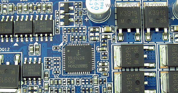
To control the power supply of the memory controller built into the processor, a 2-phase PWM controller ISL6322G is used.

The processor core is powered by a 4-phase power supply based on the ISL6334 PWM controller. In general, such a power supply should provide support for all processors in the LGA 1156 package, and also does not interfere with their moderate overclocking.

The rear panel of the GIGABYTE GA-H55M-UD2H motherboard has the following ports: one PS/2 for keyboard or mouse, optical S/PDIF, VGA and DVI video outputs, HDMI and DisplayPort high-definition interfaces, IEEE 1394a port, six USB ports, eSATA, RJ45 connector for network connections, as well as six connectors for 8-channel audio.

One of the disadvantages of the GIGABYTE GA-H55M-UD2H is the presence of only two fan connectors. Both fan headers are 4-pin, which means they support PWM power mode.
BIOS of the GIGABYTE GA-H55M-UD2H motherboard based on the Award code with a fairly wide range of settings with which you can overclock the system.

All the settings necessary for overclocking are located in the “MB Intelligent Tweaker (M.I.T.)” section, and the settings are divided into groups. In addition, this section monitors some system parameters, such as processor and memory frequencies, processor and chipset temperatures, as well as the current voltage on the processor and memory.
The settings required for overclocking are summarized in the table:
|
Parameter |
Menu name |
Range |
|
|
Processor technologies |
C1E, TM2, EIST, Virtualization Technology, |
||
|
QPI bus multiplier |
|||
|
CPU multiplier |
|||
|
Frequency system bus, MHz |
|||
|
Memory divider |
System Memory Multipllier (SPD) |
||
|
PCI Express Bus Frequency |
PCI Express Frequency |
||
|
Proprietary dynamic overclocking technology |
Cruise, Sports, Racing, Turbo, Full Thrust |
||
|
Processor signal amplitude |
700, 800, 900, 1000 mV |
||
|
PCI Express bus signal amplitude |
PCI Express Clock Drive |
700, 800, 900, 1000 mV |
|
|
RAM Latency |
CAS Latency, tRCD, tRP, tRAS, tRRD, tWTR, tWR, tWTP, tRFC, tRTP, tRAW, CMD, tRD |
||
|
CPU voltage, V |
0.50000 - 1.9 V |
||
|
QPI/Vtt bus voltage, V |
|||
|
Northbridge voltage |
|||
|
PLL supply voltage |
|||
|
Integrated GPU voltage |
CPU VAXG Voltage |
||
|
Voltage on memory modules, V |
|||
|
DRAM Termination |
|||

The number of settings in the BIOS of the GIGABYTE GA-H55M-UD2H motherboard is really very large.

The “Advanced Core Features” section contains settings for managing processor technologies.

Among all the settings, we can highlight the ability to change the QPI bus multiplier. Unlike motherboards based on Intel P55 Express system logic, there are much more multipliers, which allows you to more accurately determine its frequency during overclocking.

The GIGABYTE GA-H55M-UD2H motherboard supports XMP profiles for overclocking RAM modules, although their use is not required.
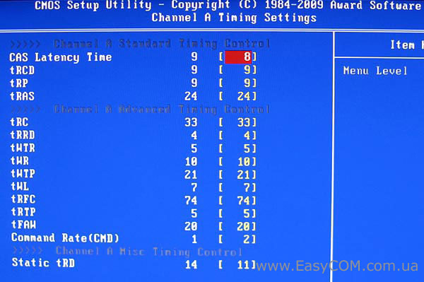
Also in the BIOS it is possible to configure RAM timings and sub-timings in full.

The number of settings designed to increase the supply voltage of components is also sufficient for good overclocking.

For example, the voltage on the processor can be increased to 1.9 V, which in some cases will be more than enough. Moreover, it is gratifying that critical and high voltage values are wisely highlighted in bright colors.

The voltage on the chipset can be increased up to 1.5 V. This voltage value is even excessive for the Intel H55 Express chipset, on which the supply voltage can not be increased or increased only slightly even with very strong overclocking of the processor.
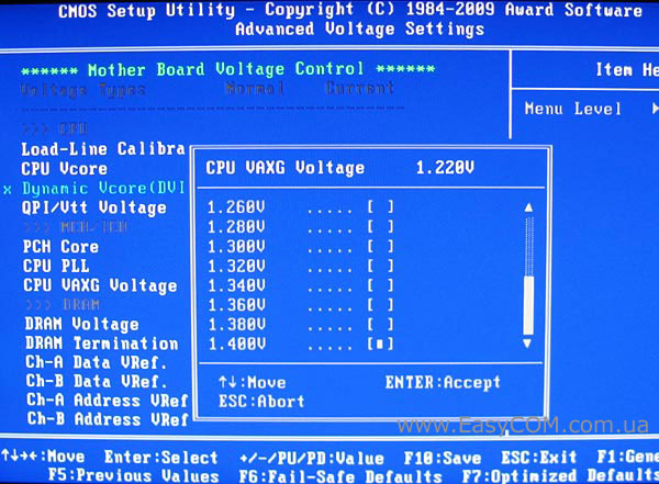
One more new setting, which can be highlighted is CPU VAXG Voltage, which allows you to increase the supply voltage on the integrated GPU.

In the monitoring section “PC Health Status” you can monitor:
- temperature of the motherboard and processor;
- rotation speed of the processor cooler and case fan;
- voltage on the processor core and RAM;
- voltage on power lines +5 V and +12V.
In addition, in this section you can enable the automatic control function CPU cooler CPU Smart FAN Control. Unfortunately, automatic control The rotation speed of the case fan is not provided.
Overclocking options

System bus clock speed of the GIGABYTE GA-H55M-UD2H motherboard with Intel processor Core i7 661 was increased to 230 MHz.
Testing
The following equipment was used to test the capabilities of motherboards.
|
CPU |
Intel Core i5 661 (LGA1156, 3.33 GHz, L3 4 MB) |
|
Scythe Kama Angle Rev. B |
|
|
RAM |
2x DDR3-2000 1024 MB Kingston HyperX KHX16000D3T1K3/3GX |
|
Video card |
ASUS EN9800GX2/G/2DI/1G GeForce 9800 GX2 1GB GDDR3 PCI-E 2.0 |
|
Hard drive |
Seagate Barracuda 7200.12 ST3500418AS, 500 GB, SATA-300, NCQ |
|
Optical drive |
ASUS DRW-1814BLT SATA |
|
power unit |
Seasonic SS-650JT Active PFC, 650 W, 120 mm fan |
|
CODEGEN M603 MidiTower, 2x 120 mm in/out fans |
Test results:


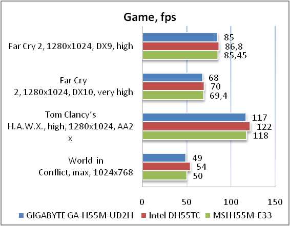
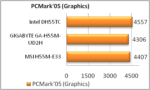
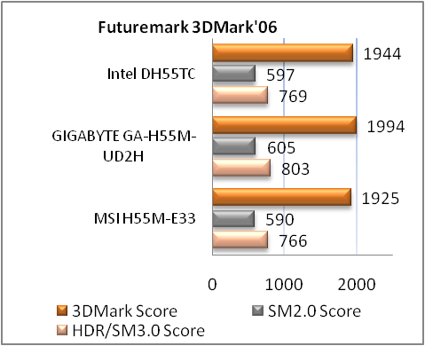
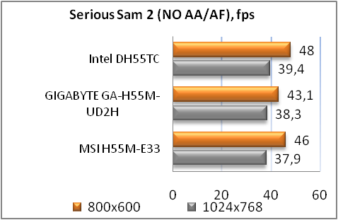
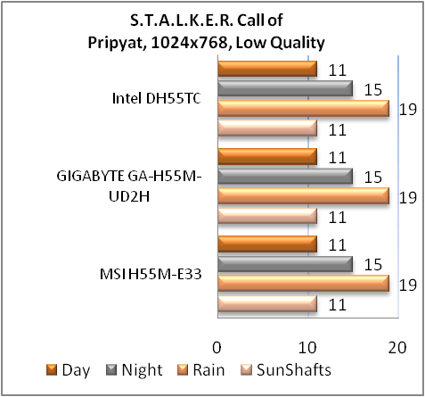
Performance testing results on the GIGABYTE GA-H55M-UD2H motherboard were slightly worse than on the Intel DH55TC motherboard. It’s difficult to say what this is connected with, since the main parameters on both systems were the same (checked several times): or the Intel board uses hidden possibilities, or for products from other manufacturers should be expected updated versions BIOS.
Working with integrated video

A similar picture is observed when testing the integrated GPU: there is a slight difference in the performance of the GIGABYTE GA-H55M-UD2H and the Intel DH55TC, and not in favor of the first.
Energy consumption
|
Energy consumption, W |
|||
|
GIGABYTE GA-H55M-UD2H + Intel Core i5-661 |
Intel DH55TC + Intel Core i5-661 |
ASUS M4A785TD-V EVO + AMD Phenom II X3 720 |
|
|
Simple (no load) |
|||
|
Stress load on the integrated video core (FurMark) |
|||
|
Stress load on the processor and integrated video core (EVEREST + FurMark) |
|||
The system based on the GIGABYTE GA-H55M-UD2H motherboard has higher power consumption than the similar system based on the Intel DH55TC motherboard. This happens primarily because by default the GIGABYTE GA-H55M-UD2H sets the processor supply voltage to a higher value. Secondly, it is equipped with a large number of controllers, which also slightly increase power consumption.
Competing AMD platform with AMD processor The Phenom II X3 720 and a motherboard based on AMD 785G system logic with an integrated Radeon HD4200 video core have higher power consumption, but its cost in this case will be lower.
Testing the audio path based on the Realtek ALC889 codec
Overall results (RightMark Audio Analyzer)
16-bit, 44.1 kHz
The built-in Realtek ALC889 audio codec shows very good results, so we think it will be enough for the vast majority of owners.
Conclusions
The GIGABYTE GA-H55M-UD2H motherboard can be a good basis for a work, multimedia or even gaming system. This model supports a number of GIGABYTE proprietary technologies (UltraDurable 3, Smart 6), has a FireWire controller, is equipped with a high-quality audio codec and supports four types of video outputs. This allows you to connect any monitor to it. In the BIOS of the GIGABYTE GA-H55M-UD2H motherboard you can find a very large number of settings necessary for overclocking with a wide control range and small steps. The only thing that will not contribute to high overclocking results is not the most powerful processor power regulator with a 4-pin ATX12V power connector. In the GIGABYTE model range based on the Intel H55 Express chipset, there are also models with a more powerful power supply unit, so if you are interested in overclocking, you should pay attention to the GIGABYTE GA-H55M-USB3 or GIGABYTE GA-H57M-USB3, which in addition have USB support 3.0. If serious overclocking is not expected and there is a desire or need to save a little, then the GIGABYTE GA-H55M-UD2H will be a good choice.
Sea Sonic for providing test bench equipment.
Article read 30207 times
| Subscribe to our channels | |||||
|
|
|
||||
We recently conducted a comparative test of boards based on the Intel H55/H57 chipset, where we complained about the lack of inexpensive entry-level boards. And almost immediately after that we received for testing the ASRock H55M-LE model on the Intel H55 chipset, the cost of which is very low. Of course, the price reduction did not happen just like that. The fact is that the company's engineers reduced the number of USB 2.0 ports from twelve to ten, and the number of SerialATA II channels was reduced from six to four. Whether such a reduction in functionality justifies the reduction in the price of the board, we will try to figure it out in this review.
⇡ ASRock H55M-LE Specification
| CPU | - Intel Core i7/Core i5/Core i3 Bclk 133 MHz - LGA1156 connector - Support Intel technologies Turbo Boost |
| Chipset | - Intel H55 (PCH) - Communication with processor: DMI |
| System memory | - Two 240-pin DDR3 SDRAM DIMM slots - Maximum memory 8 GB - Supports memory type DDR3 1066/1333/1600*/1866*/2133*/2600* - Dual channel memory access possible - Intel XMP technology support |
| Graphics | - One PCI Express x16 slot - Intel support HD Graphics (with matching processor) |
| Expansion options | - Two 32-bit PCI Bus Master slots - One PCI Express x1 slot - Ten USB 2.0 ports (six built-in + four additional) - High Definition Audio 7.1 sound - Gigabit Ethernet network controller |
| Overclocking options | - Changing the Bclk frequency from 100 to 300 MHz in 1 MHz steps; CPU multiplier change - GPU frequency change up to 1333 MHz - Change voltage on CPU, PLL, memory, IMC, ViGPU and chipset - OC Tuner utility |
| Disk subsystem | - Support for SerialATA II protocol (four channels - Intel H55) |
| BIOS | - 16 Mbit Flash ROM - AMI BIOS with support for Enhanced ACPI, DMI, Green, PnP Features - ASRock Instant Flash Technology - ASRock OC DNA technology |
| Miscellaneous | - One serial and one parallel port, PS/2 keyboard port - STR (Suspend to RAM) - SPDIF Out |
| Power management | - Wake from modem, mouse, keyboard, network, timer and USB - Primary 24-pin ATX power connector - Additional 4-pin power connector |
| Monitoring | - Monitoring the temperature of the processor, system, monitoring voltages, determining the rotation speeds of all fans (three); - SmartFan technology - ASRock I.E.S technology (Intelligent Energy Saver) |
| Dimensions | - MicroATX form factor, 244x203 mm (9.6" x 8.0") |
The ASRock H55M-LE motherboard box looks like this:
⇡ Equipment
The delivery set includes the following items:
- motherboard;
- user manual;
- DVD with software and drivers;
- two SerialATA cables;
- plug for the rear panel of the case.
The package package of the ASRock H55M-LE board is the poorest we have ever seen (not counting Intel boards DH55TC). This is expressed both in the minimum number of components and in scant documentation. The user manual itself is thick, but only 20 pages are devoted to a description of the board's characteristics, and the rest of the brochure is the same information, duplicated in many languages (including Russian). Also note that the manual does not contain a description of the BIOS settings.

However, we rate the board's packaging as "good", since the retail price of this product is around 2,500 rubles, which is the best offer today.
⇡ ASRock H55M-LE board
Due to the low price, there can be no complaints about the design of the H55M-LE board. Let us note, perhaps, the close proximity of the PEG slot and memory slots, but this cannot be considered a disadvantage, since inexpensive boards are often used with integrated graphics.

In addition to the main 24-pin power connector (located on the bottom edge), the board has an additional 4-pin:

Next to the processor socket there is a 4-pin connector for the corresponding cooler. There is also one more 4-pin and one 3-pin connector on the board.

Around the processor socket there is an additional set of mounting holes for coolers designed for the LGA775 socket. This is a big plus both for those who like to save money and for overclockers. But let’s immediately note that there is no 100% guarantee that the board will be compatible with these coolers and some models may not be suitable.
The board has two 240-pin blue DIMM slots for DDR3 memory modules. In order to use dual-channel mode, you must install modules in both slots. By the way, the board supports DDR3 memory with all possible frequencies, and the maximum total memory capacity is 8 GB.

The board has a full-featured PCI-E x16 slot, a PCI Express x1 slot, and a pair of PCI slots.

⇡ Expansion options
The ASRock H55M-LE board has only four SerialATA II ports out of six supported Intel chipset H55. The corresponding ports are colored red and are located near the chipset.

Since the board does not support the ParallelATA interface, the total number of connected drives is four. The board has ten USB 2.0 ports: six are located on the rear panel, and four more are connected using brackets (not included). The ASRock H55M-LE board has eight-channel audio, and the VIA VT1718S chip is used as the codec.

The board also includes a high-speed network controller RTL8111DL (Gigabit Ethernet), connected to the PCI Express (x1) bus.

The corresponding connector (RJ-45) is located on the rear panel of the board, which has the following configuration:

Note that the board has only two of four possible graphics outputs. In particular, DVI and VGA outputs are located on the rear panel (HDMI and DisplayPort are missing).
Traditional component diagram:

Now let's talk about BIOS settings.
⇡BIOS
The BIOS of ASRock H55M-LE is based on the AMI BIOS version, and its size is 16 Mbit.

The board allows the user to change both memory timings and its operating frequency.


Now let's look at the section on system monitoring.

Fee Tracking current temperature processor and system, monitors voltages, determines the rotation speeds of all three fans. Also note that the user can control the speed of the fans (connected to the 4-pin connectors) using the SmartFan function.

It should be noted that the user gets access to all technologies that are supported modern processors Intel:

In addition, the board supports three BIOS profiles. The corresponding save and load functions are located in the overclocking section:

Based on this function, ASRock programmers wrote the OC DNA utility, which allows you to operate profiles like files (i.e. you can send a profile by mail, post it on the Internet, etc.).

And finally, we note the ability to adjust the amount of memory allocated for the needs of integrated graphics:

There is also a built-in BIOS firmware utility - Instant Flash:

⇡ Overclocking and stability
Before moving on to overclocking, let's take a look at the power converter. It has a 5-phase design (4+1), in which seven capacitors with a capacity of 270 μF and 13 capacitors with a capacity of 820 μF are installed.

Despite the budget design of the ASRock H55M-LE board, it supports a large number of overclocking functions.


Some of them are intended for beginner overclockers and are quite easy to use. These are "CPU EZ OC Settings", "Memory EZ OC Settings", "GPU EZ OC Settings":


Their meaning is that the user selects the desired overclocking level - and the board sets all the appropriate settings. In fact, we have an analogue of the ASUS CPU/Memory LevelUP functions, but the overclocking process is far from ASUS quality. In particular, if the settings are too aggressive, the system freezes so that it can only be revived using the BIOS reset jumper. Another drawback - incorrect operation the "GPU EZ OC Settings" function, which is responsible for increasing the frequency of the graphics core.
As for the "Turbo" function, it is probably a generalized function that increases the frequencies of the processor, memory and graphics core at the same time. Unfortunately, with our test set of components, this feature caused the system to freeze.

Other overclocking functions:
| Pay | ASRock H55M-LE |
| Changing the CPU multiplier | + |
| Change Bclk | 100 MHz to 300 MHz (1 MHz) |
| Changing GPUclk | 133 MHz to 1333 MHz (33 MHz) |
| Vcore change | 0.84375 V to 1.6 V (0.00625 V) |
| Vmem change | 1.3 V to 2.05 V (0.05 V) |
| Changing Vimc | 1.05 V to 1.55 V (~0.06 V) |
| Change Vpll | 1.81 V to 2.18 V (~0.12 V) |
| Vpch change | 1.05 V to 1.25 V (0.1 V) |
| Changing ViGPU | 0.85 V to 1.4625 V (0.0125 V) |
Practical experiments showed the following results: stable operation at a Bclk frequency of 182 MHz.

As for overclocking the graphics core built into the processor, the board allows you to change its frequency within a fairly wide range:

In our case, the system worked stably up to a frequency of 1 GHz:

And finally, we note the OC Tuner utility, which, in addition to the main task, performs a number of secondary ones (for example, displaying system monitoring data).

We also mention the “energy conservation” technology called IES (Intelligent Energy Saver).

⇡ Performance
When determining the starting frequency of Bclk, it turned out that the board overestimates it by five (!) MHz (with all settings set to default):

Therefore, to determine the performance of the board, we had to forcefully fix Bclk frequency at 133 MHz:

IN test system The following equipment was used:
|
Test bench |
|
|---|---|
| CPU | Processor Intel Core i3 530 (LGA1156; 2.93 GHz; Clarkdale core) |
| Cooler | Boxing |
| Video card | Intel HD Graphics |
| Sound card | - |
| HDD | Samsung HD160JJ |
| Memory | 2x 1024 MB |